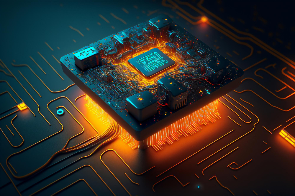
Revolutionizing electronic manufacturing: Advanced PCBs and the role of nano printing
The electronics in today’s world are spreading into new applications daily, improving our lives. From extremely capable smartphones and wearable electronics through complex industrial control modules to simple household items like an electric kettle. Among others- two conclusions can be drawn from this. One is that electronics will need to be further reduced in size to allow them to be assimilated into devices. The second is that the global production volumes will only go up to satisfy the market demands. Advanced PCB design answers the first point- they allow for increased packaging density on the board and, in some cases, enable flexibility. Conductive ink for PCB with nano inks enhances the ability to design and use additive PCB manufacturing. What previously was either unacceptable in terms of prototype timing or prohibitively expensive is now – with nanoparticle (NP) paste-like XTPL’s CL85, it is possible for rapid PCB prototyping or small-scale production in an additive process.
Limitations of Traditional PCB Manufacturing
Traditional PCB manufacturing is based on etching, lamination, and drilling, which do not support the industry drive for certain aspects. This includes a lack of better heat management options when reducing the size and increasing circuit voltage. A growing number of electronic applications in IoT, medical sensors, and especially wearables dictate that PCBs must evolve into more specialized branches. A designer with high packaging requirements will need to look for more innovative manufacturing techniques with several possible layers, another designer for a medical application will select a flexible board, and an R&D engineer for a semicon company will look for a fast prototype pcb manufacturing method. All that is less and less achievable with traditional PCB manufacturing.
The Promise of Advanced PCB Design
Advanced PCB design offers solutions for these challenges. This includes the promise of lower power consumption, improved signal quality, and reduced dimensional deviations with the possibility of size reduction in multilayer designs. More compact sizes allow for reduced weight, which is always getting more and more attention for mobile applications. Multilayer PCB also makes possible, though not in all cases, a flexible design with a specific yield infused with proper advanced circuits and flex PCB construction techniques. Increased durability also lies in the DNA of advanced PCBs- they offer excellent heat handling capabilities, which are very much needed when tightly integrated and packaged (bear in mind the reduced size of mobile and wearable devices). Consumer electronics, automotive, and healthcare industries drive the change in requirements in a direction that mandates a decrease in size and weight, promoting wearability and portability. The miniaturization of electronics also allows innovative capabilities to be tagged into new household devices, enlarging the IoT market size and enabling the capability to satisfy end consumer needs. Increased efficiency, ability and potential open new technology limits for 5g and, shortly, 6g.
The Rise of Nano Printing for PCB Manufacturing
A new technology had to emerge to cover all the stringent requirements for advanced circuits PCB. One is nano printing, an additive process where nanoparticles are delivered onto a substrate to obtain a conductive filament on PCB. This process gives unparalleled flexibility as you can use it with extremely high resolution – in the case of XTPL’s UPD technology, the feature can be as narrow as 1 µm with precision between features as low as few µm (this extremely important when comparing to inkjet where resolution is limited because of overspray- the features will not present a uniform distance between them), virtually on any substrate. Evoked technology is exceptionally beneficial for PCB fast prototyping without elaborate and expensive tooling; the organization can achieve incredibly intricate advanced assembly PCB.
The Application of Additive PCB Manufacturing
Once again, the application area of components made in additive PCB manufacturing, let’s re-iterate reduced weight and dimensions- span over many industries. Exceptionally wearable electronics and smart textiles where conductive ink, like for PCB, is seamlessly integrated with the yarn to provide new functions never seen directly on a piece of clothing. Biomedical applications for lab on chips, precise electrodes for sensors and, in this case, conductive inks from gold have confirmed biocompatibility- even implantable biosensors.
Challenges and Future Prospects of Advanced PCBs and Nano Printing
Despite the many advantages above, there are also a lot of challenges. One of them is process optimization and scalability in the case of technologies currently exploited in more r/d style use cases. However, now limited- without a doubt, in the future, this will be ironed out as the industry adapts to new technology. This, for sure, will be driven by the electronic manufacturing industry; there is no question if a fast prototype PCB process is needed to accelerate product development cycles. Lack of tooling will improve the ability of small enterprises and startups to compete in the microelectronics world. This will be constantly improved by pushing the boundaries by integrating novel materials or flexible electronics.
Nano printing and advanced PCBs go hand in hand, guiding us into tomorrow’s future (seemingly) limitless applications, creating new manufacturing techniques and new types of devices that will be commonly available for consumers and improve our lives. The industry will have to invest further in technology to unsettle the unimaginable devices of the future.